
SK Hynix and Samsung Electronics plan to expand production of HBM memory on a large scale this year, although currently only achieving a yield rate of 65%
HBM memory adopts wafer level packaging (WLP) technology, which connects multiple layers of DRAM memory wafers through TSV silicon through holes. Among them, a problem with one layer of DRAM resulted in the entire HBM stack being scrapped. Taking 8-layer stacked products as an example, if the yield of each stack is 90%, the overall yield of the HBM stack is only 43%, and more than half of the DRAM is discarded. As the number of HBM layers increases, such as entering the 12 or 16 layer stack, the yield further decreases.
Currently, DealSite reports that the overall yield of HBM memory is only about 65%, significantly lower than traditional memory products. Due to the nature of WLP, it is difficult to increase yield to 80% or 90%.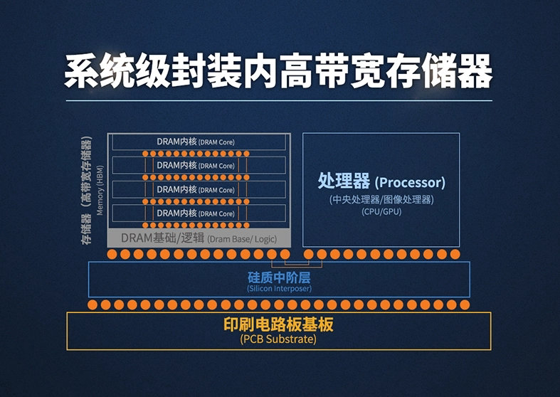
On the other hand, SK Hynix and Samsung Electronics, as leading manufacturers in the HBM memory market, are both significantly expanding their production capacity this year. According to Kiwoom Securities, a South Korean securities firm, Samsung Electronics' monthly HBM memory production capacity is expected to increase from 25000 wafers in the second quarter of last year to 15.17 million wafers in the fourth quarter of this year; At the same time, SK Hynix's monthly production capacity is expected to jump from 35000 pieces to 12.14 million pieces. This shows that while facing challenges, the two major manufacturers are also actively responding to market demand to meet the growing semiconductor market.
However, compared to the demand for HBM memory in the AI market, the capacity growth of SK Hynix and Samsung is still insufficient: SK Hynix executives have once again confirmed that the HBM capacity quota has been sold out this year; According to a report by South Korean media NEWSIS at the end of last year, Samsung has already completed negotiations with major customers regarding this year's production capacity.
Mobile number: 13510285528
e-mail address: 13510285528@139.com
Enterprise QQ: 2880981362
Headquarters Address: 1201, Block A, Jiahe Huaqiang Building, No. 3006 Shennan Middle Road, Futian District, Shenzhen, Guangdong Province
HK Company: Room D, 16th Floor, Hyde Centre, 18 Luang Road, Wan Chai, Hong Kong

