
Intel officially announces large-scale production of 3D advanced packaging technology Foveros
This technology was launched in the latest upgraded Fab 9 from New Mexico, USA. Keyvan Esfarjani, Executive Vice President and Chief Global Operations Officer of Intel, said, "Advanced packaging technology sets Intel apart, helping our customers gain competitive advantages in chip product performance, size, and flexibility in design applications.".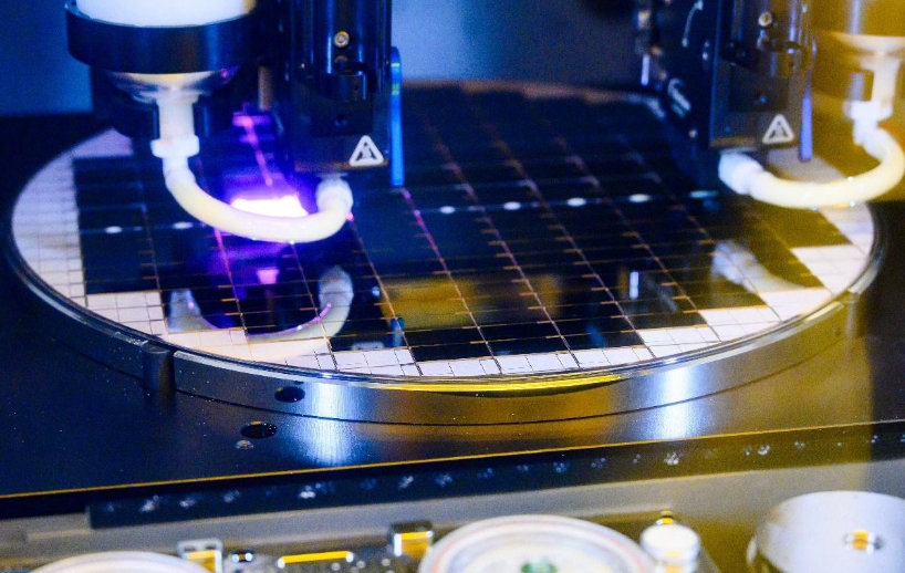 As the entire semiconductor industry enters a heterogeneous era of integrating multiple "chips" in a single package, Intel's advanced packaging technologies such as Foveros and EMIB (Embedded Multi Chip Interconnection Bridge) claim to be able to integrate one trillion transistors in a single package and continue to advance Moore's Law after 2030. It is reported that Intel's 3D advanced packaging technology Foveros can stack computing modules vertically rather than horizontally in the manufacturing process of processors. In addition, Foveros enables Intel and its foundry customers to integrate different computing chips, optimize costs and energy efficiency.
 The company has stated that it plans to increase its 3D Foveros packaging capacity fourfold by 2025.
Mobile number: 13510285528
e-mail address: 13510285528@139.com
Enterprise QQ: 2880981362
Headquarters Address: 1201, Block A, Jiahe Huaqiang Building, No. 3006 Shennan Middle Road, Futian District, Shenzhen, Guangdong Province
HK Company: Room D, 16th Floor, Hyde Centre, 18 Luang Road, Wan Chai, Hong Kong

